- 您现在的位置:买卖IC网 > Sheet目录325 > FAN73833MX (Fairchild Semiconductor)IC HALF BRIDGE GATE DRIVER 8-SOP
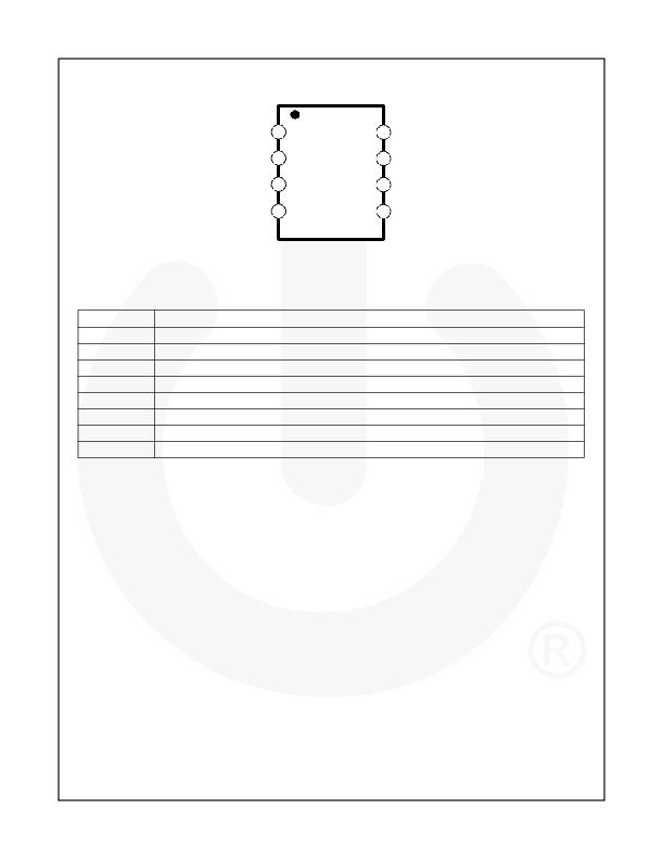
Pin Configuration
LIN
HIN
V DD
COM
1
2
3
4
8
7
6
5
V B
HO
V S
LO
Figure 3. Pin Configuration (Top View)
Pin Definitions
Pin #
1
2
3
4
5
6
7
8
Name
LIN
HIN
V DD
COM
LO
V S
HO
V B
Description
Logic Input for Low-Side Driver
Logic Input for High-Side Driver
Low-Side Supply Voltage
Logic Ground and Low-Side Driver Return
Low-Side Driver Output
High-Side Floating Supply Return
High-Side Driver Output
High-Side Floating Supply
? 2008 Fairchild Semiconductor Corporation
FAN73833 ? Rev.1.0.2
3
www.fairchildsemi.com
发布紧急采购,3分钟左右您将得到回复。
相关PDF资料
FAN7383MX
IC GATE DVR HALF BRIDGE 14-SOIC
FAN7384MX
IC DRIVER GATE HALF BRIDGE 14SOP
FAN7385MX
IC GATE DRIVER HISIDE 2CH 14-SOP
FAN7388MX
IC GATE DRIVER HALF BRIDG 20SOIC
FAN73892MX
IC GATE DVR HALF BRDG 3PH 28SOIC
FAN7389MX
IC GATE-DRIVE 3PH HALFBRDG 24SOP
FAN73901M
IC GATE DRIVER HI/LOW SIDE 8SOIC
FAN7390M1X
IC DRIVER GATE HI/LO SIDE 14-SOP
相关代理商/技术参数
FAN7383M
功能描述:功率驱动器IC Half Brige Gate RoHS:否 制造商:Micrel 产品:MOSFET Gate Drivers 类型:Low Cost High or Low Side MOSFET Driver 上升时间: 下降时间: 电源电压-最大:30 V 电源电压-最小:2.75 V 电源电流: 最大功率耗散: 最大工作温度:+ 85 C 安装风格:SMD/SMT 封装 / 箱体:SOIC-8 封装:Tube
FAN7383MX
功能描述:功率驱动器IC Half Bridge Gate Driver RoHS:否 制造商:Micrel 产品:MOSFET Gate Drivers 类型:Low Cost High or Low Side MOSFET Driver 上升时间: 下降时间: 电源电压-最大:30 V 电源电压-最小:2.75 V 电源电流: 最大功率耗散: 最大工作温度:+ 85 C 安装风格:SMD/SMT 封装 / 箱体:SOIC-8 封装:Tube
FAN7383MX_WS
功能描述:功率驱动器IC MOS DRVR 600V 0.65A 4-Out Hi/Lo RoHS:否 制造商:Micrel 产品:MOSFET Gate Drivers 类型:Low Cost High or Low Side MOSFET Driver 上升时间: 下降时间: 电源电压-最大:30 V 电源电压-最小:2.75 V 电源电流: 最大功率耗散: 最大工作温度:+ 85 C 安装风格:SMD/SMT 封装 / 箱体:SOIC-8 封装:Tube
FAN7384
制造商:FAIRCHILD 制造商全称:Fairchild Semiconductor 功能描述:Half-Bridge Gate-Drive IC
FAN7384_0702
制造商:FAIRCHILD 制造商全称:Fairchild Semiconductor 功能描述:Half-Bridge Gate-Drive IC
FAN7384_09
制造商:FAIRCHILD 制造商全称:Fairchild Semiconductor 功能描述:Half-Bridge Gate-Drive IC
FAN7384M
功能描述:功率驱动器IC Half Bridge Gate Driver RoHS:否 制造商:Micrel 产品:MOSFET Gate Drivers 类型:Low Cost High or Low Side MOSFET Driver 上升时间: 下降时间: 电源电压-最大:30 V 电源电压-最小:2.75 V 电源电流: 最大功率耗散: 最大工作温度:+ 85 C 安装风格:SMD/SMT 封装 / 箱体:SOIC-8 封装:Tube
FAN7384MX
功能描述:功率驱动器IC Half Bridge Gate RoHS:否 制造商:Micrel 产品:MOSFET Gate Drivers 类型:Low Cost High or Low Side MOSFET Driver 上升时间: 下降时间: 电源电压-最大:30 V 电源电压-最小:2.75 V 电源电流: 最大功率耗散: 最大工作温度:+ 85 C 安装风格:SMD/SMT 封装 / 箱体:SOIC-8 封装:Tube
